Publications
“Boosting SiC Throughput”, Compound Semiconductor Magazine, Special Issue: SiC manufacturing. September 2021.
“Impact of Reduced Gate-to-Source Spacing on InP HEMT Performance” Physica Status Solidi A, Special Issue: Compound Semiconductors. October 2020.
“Low-Noise Microwave Performance of 30 nm GaInAs MOS-HEMTs: Comparison to Low-Noise HEMTs”. IEEE Electron Device Letters. September 2020.
“Effects of Electrochemical Etching on InP HEMT Fabrication”. IEEE Transactions on Semiconductor Manufacturing. September 2019.
“InAs Channel Inset Effects on the DC, RF, and Noise Properties of InP pHEMTs”. IEEE Transactions on Electron Devices. October 2019.
“Pt Gate Sink-In Process Details Impact on InP HEMT DC and RF Performance”. IEEE Transactions on Semiconductor Manufacturing. September 2017.
“Evaluation of energy barriers for topological transitions of Si selfinterstitial clusters by classical molecular dynamics and the kinetic activation-relaxation technique”. Conference of Electron Devices (CDE 2017). Conference Proceedings.
“Aplicaciones e-Health y Dispositivos Wearables: Revolución Inminente”. Magazine CyL Digital (3er cuatrimestre 2014 - Nº13). September 2014.
Jornal Articles


Conferences
“Novel Vitrified-bond Ultra-fine Grinding Technology for SiC Polishing”, 13th European Conference on Silicon Carbide and Related Materials (ECSCRM 2020·2021), Tours (France), October 2021.
“Gate Annealing Effect on the Cut-off Frequencies and Noise Performance in InP based GaInAs Depletion-Mode MOSHEMT” 44th Workshop on Compound Semiconductor Devices and Integrated Circuits (WOCSDICE 2020), Bristol (UK), June 2020.
“Impact of Reduced Gate-to-Source Spacing on InP HEMT Performance” 2020 Compound Semiconductor Week (CSW 2020), Stockholm (Sweden), May 2020.
“Gate Recess Etch Sensitivity of Thick and Highly-Doped GaInAs Cap Layer in InP HEMT Fabrication” International Conference on Compound Semiconductor Manufacturing Technology (CS ManTech 2020), Tucson (US), May 2020.
“Impact Ionization Control in 50 nm Low-Noise High-Speed InP HEMTs with InAs Channel Insets”. 65th IEEE International Electron Devices Meeting (IEDM 2019), San Francisco (US). December 2019.
“New GaInAs/InAs/InP Composite Channels for mm-Wave Low-Noise InP HEMTs”. IEEE BiCMOS and Compound Semiconductor Integrated Circuits and Technology Symposium 2019 (BCICTS 2019), Nashville (US). November 2019.
“Effects of Electrochemical Etching on InP HEMT Fabrication”. International Conference on Compound Semiconductor Manufacturing Technology (CS ManTech 2019), Minneapolis (US). May 2019.
“Pt Gate Sink-In Process Details Impact on InP HEMT DC and RF Performance”. International Conference on Compound Semiconductor Manufacturing Technology (CS ManTech 2017), Indian Wells (US). May 2017.
“Evaluation of energy barriers for topological transitions of Si selfinterstitial clusters by classical molecular dynamics and the kinetic activation-relaxation technique”. Conference of Electron Devices (CDE 2017), Barcelona (Spain). February 2017.
“Characterization and dynamics of Si self-interstitial clusters by self-learning kinetic Monte Carlo simulations”. European School on Molecular Nanoscience 2016 (ESMolNa 2016), Tordesillas (Spain). June 2016.
“Molecular dynamics simulations of intrinsic defects in amorphous Ge”. Conference on Gettering and Defect Engineering in Semiconductor Technology 2015 (GADEST 2015), Bad Staffelstein (Germany). September 2015.
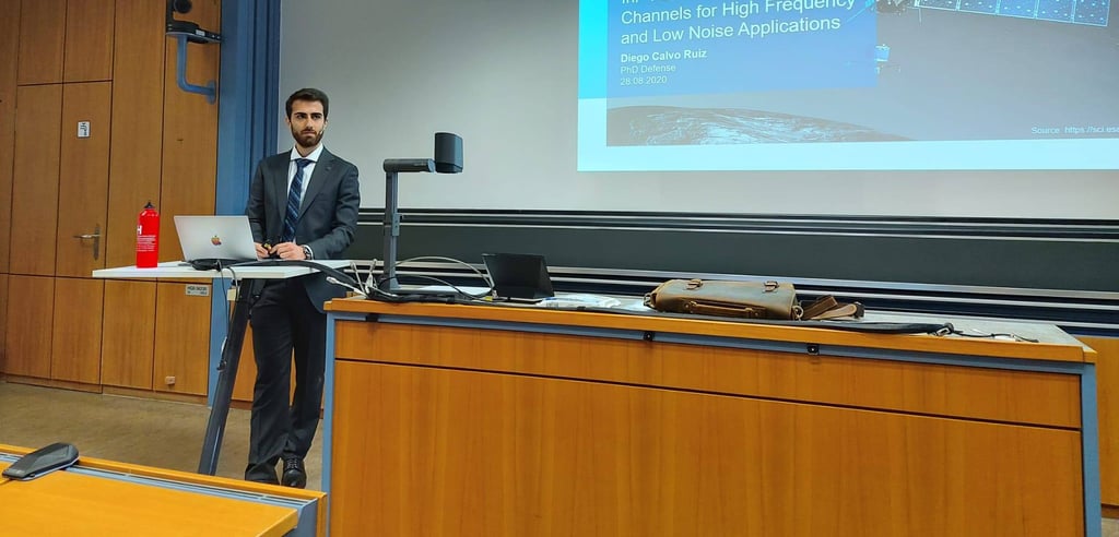
Over the last years I have given several talks in front of a wide variety of audiences in the US and Europe mainly.
